How Quantum Mechanics Powers the Transistor
Transistors work because of quantum effects like tunneling and energy levels.

Abstract
Transistors work because of quantum effects like tunneling and energy levels. This blog explains the theory, how it’s used today, and one central area where transistor tech can still improve.
***Warning: this is a very nerdy post. I have narrowed a graduate-level class into a blog post of fewer than 750 words. Please message me if I get something wrong so that I can correct it.
How Quantum Mechanics Powers the Transistor
When you hear “quantum mechanics,” you might picture Star Trek or supercomputers. But the truth is way more straightforward—and way cooler. Quantum physics is quietly running your everyday life. It’s inside your phone, your laptop, your TV, and almost every electronic device you touch.
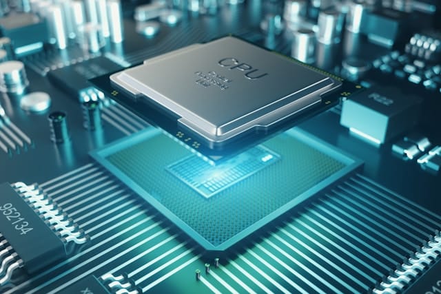
At the heart of all of this is the transistor, a tiny electrical switch that turns current on and off. Billions of these switches live inside a single processor. And the only reason they work is because of quantum mechanics.
Tunneling and Energy Levels
To understand transistors, you need two key quantum ideas:
Quantized Energy Levels
Electrons can’t just have any amount of energy. Instead, they live in specific energy levels, like steps on a staircase. If an electron doesn’t have enough energy to jump to the next step, it simply can’t.
Semiconductors—materials used to make transistors—depend on this rule. They have a band gap, an energy “no-go zone” between two levels. Electrons need just the right amount of energy to cross it.
Quantum Tunneling
In the everyday world, if you don’t have the energy to climb a hill, you stay put. But in the quantum world, particles can sometimes do something wild: they can “tunnel” through barriers they shouldn’t have the energy to cross.
This is called quantum tunneling, and it becomes more likely as the barrier gets thinner.
As engineers shrink transistors ever smaller, the physical barriers inside them get thinner too, and that means tunneling becomes a significant factor in how electricity behaves on a chip.
How This Is Applied in Today’s Technology
A transistor has three main parts: the source, drain, and gate. The gate acts like a valve. Apply voltage, and electrons get the energy needed to cross the band gap and flow. When the voltage is removed, electrons fall back to lower energy levels and stop.
This “on/off” behavior made possible by quantized energy levels is the fundamental language of computers: 1s and 0s.
Now layer on quantum tunneling:
When transistors get extremely small, electrons can tunnel through the barriers—even when the transistor is supposed to be “off.”
Modern chip designs must account for this because tunneling can cause leakage current, wasted power, and heat buildup.
Today’s cutting-edge chips, like those in high-end smartphones and laptops, use FinFET or GAAFET designs that reduce unwanted tunneling while still allowing billions of transistors to fit on a tiny chip.
One Area That Needs Improvement
The biggest challenge? We’re reaching the limits of how small transistors can get.
As they approach atomic scale thickness:
Tunneling becomes harder to control
Heat becomes more complicated to manage.
Power leaks increase
Reliability decreases
The next significant improvement is from new materials, such as graphene or 2D semiconductors, or from entirely new transistor structures that handle quantum effects more gracefully.
I have already started writing my next blog based on the information I learned while writing this one. So stay tuned.
Buy me a coffee at:
https://buymeacoffee.com/clubtj
Visit my blog at:
https://www.quarkstochlorophyll.blog
Credit where due:
https://www.youtube.com/watch?v=TxUqxHA2NG81
https://www.youtube.com/watch?v=oPwd5bNMo0Q
https://www.youtube.com/watch?v=_mVBbdbqHmw&t=15s
© 2025 Tim Jackson. All Rights Reserved.